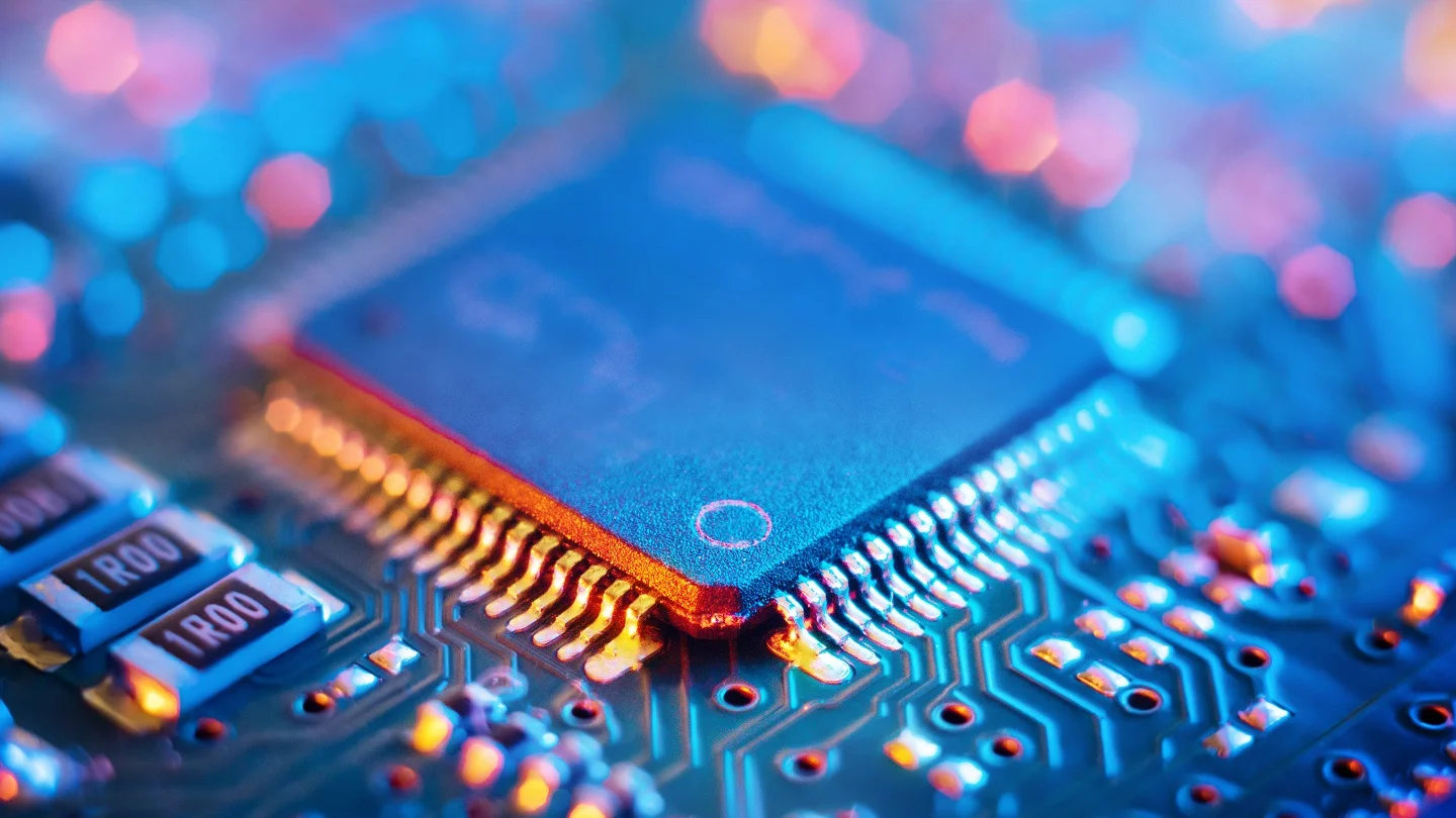
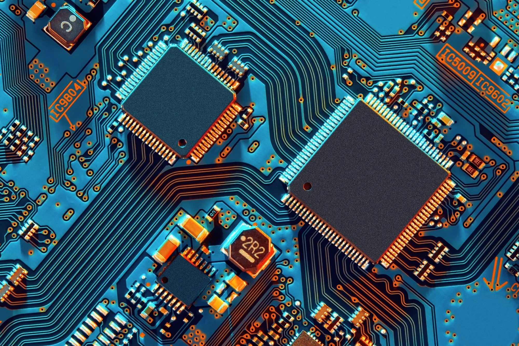
Semiconductor Solutions
Specifically developed soldering solutions for semicon processes such as Die Attach, Ball Attach (CSP, BGA), flip chip and waferbumping, POP & SIP.
Select subsegment :
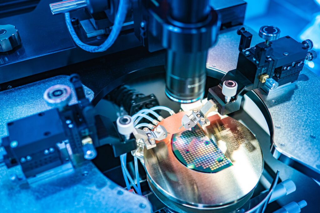
Ball Attach
Ball attach is a useful process in the semiconductor manufacturing industry, specifically for attaching solder balls to substrates, wafers, or PCBs, which is essential to produce integrated circuits (ICs) and microelectronics.
INVENTEC offers soldering solutions in the semiconductor sector that provide advanced chemical products enabling the perfect attachment of solder balls.
These soldering products must meet stringent standards for thermal conductivity, mechanical strength, and electrical performance to ensure the longevity and functionality of semiconductor devices. Specialized fluxes, pastes, and solder alloys are formulated for optimal ball attach, ensuring strong, durable, and consistent joints in the final product.
Read moreRelated products & services
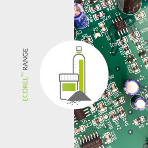
ECOFREC TF48

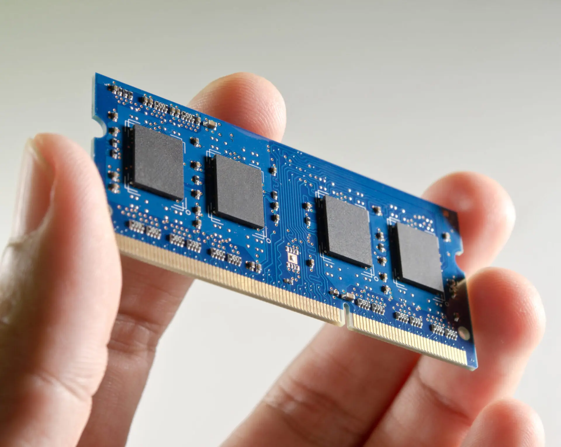
Die Attach
Die attach is an important process in semiconductor manufacturing. It involves the precise attachment of a semiconductor die to a substrate or package, playing a pivotal role in ensuring the performance, reliability, and durability of semiconductor devices.
INVENTEC offers soldering solutions, especially through innovative chemical products, making us a key player in the die attach process.
Advanced die attach materials, including conductive adhesives, silver sintering pastes, and lead-free solders, are widely used in the semiconductor industry to ensure optimal thermal and electrical conductivity, as well as long-term stability in the harsh operating conditions of semiconductor devices.
Read moreRelated products & services
ECOREL HT 301T
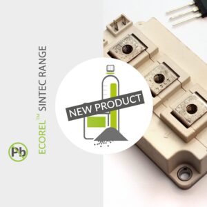
ECOREL SINTEC XP95D
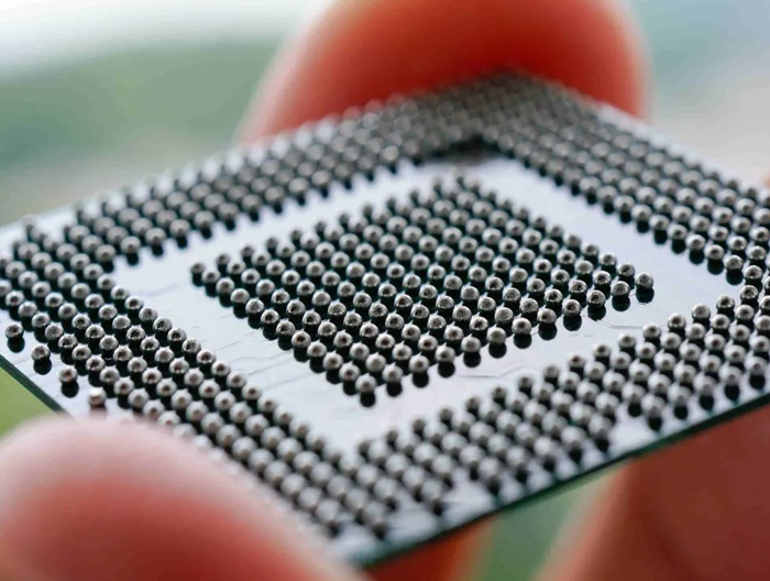
Flip Chip & CSP
Flip Chip and CSP (Chip-on-Substrate) technologies are important in SMT solder paste applications as they enable high-density interconnects and improved electrical performance, supporting miniaturization and enhanced reliability in advanced electronic assemblies.
In the rapidly evolving semiconductor industry, Flip Chip and CSP (Chip-on-Substrate Packaging) technologies have revolutionized the way electronic components are assembled and integrated.
Flip Chip packaging is a critical advancement, enabling a more compact design with improved performance by flipping the chip upside down and connecting it directly to the substrate via solder bumps. This approach enhances thermal and electrical conductivity, making it ideal for high-performance semiconductor solutions used in advanced applications.
INVENTEC offering of soldering solutions for the semiconductor sector plays a crucial role in ensuring the reliability and efficiency of these technologies, with products designed to optimize the process and reduce defects.
Read moreRelated products & services
ECOFREC POP WS30

ECOFREC TF48
PoP Assembly
PoP (Package-on-Package) Assembly plays a key role in SMT (Surface-Mount Technology) solder paste application by ensuring precise alignment and reliable soldering of stacked components, enhancing space efficiency and electrical performance in compact electronic devices.
PoP (Package on Package) Assembly is a critical process in the semiconductor industry, particularly when it comes to optimizing space and performance in advanced electronic devices. This assembly method involves stacking multiple IC (Integrated Circuit) packages on top of one another, creating a compact and efficient solution for applications such as smartphones, tablets, and other high-performance electronics.
In PoP assembly, high-precision soldering is essential, and specialized soldering solutions, often involving advanced solder pastes and fluxes, are used to ensure reliable connections between stacked packages. These soldering solutions are developed to meet the rigorous demands of the semiconductor sector, ensuring consistency, high yield, and minimizing defects during the assembly process.
INVENTEC, offering soldering solutions and supplying these materials with precise chemical formulations tailored for PoP assembly is crucial to achieving optimal results in the semiconductor solutions sector. By focusing on providing high-performance soldering materials, manufacturers can ensure that their PoP assemblies meet the highest standards for reliability, durability, and performance.
Read more
Related products & services
ECOREL HT 301T
ECOFREC POP WS30
System-in-Package (SIP)
System-in-Package (SIP) technology enhances SMT solder paste applications by integrating multiple components into a single package, improving compactness, performance, and reliability in modern electronic devices.
System-in-Package (SIP) technology is a revolutionary approach in the semiconductor industry, combining multiple integrated circuits (ICs) into a single package to enhance performance, reduce size, and improve efficiency.
INVENTEC offers soldering solutions in the Semicon Solutions sector, playing a vital role in the SIP process by providing specialized chemical products such as advanced solders, fluxes, and underfills.
These soldering materials are crucial for ensuring reliable interconnections between the various components within a SIP, ensuring long-term durability and performance under demanding conditions. The precision and quality of these soldering solutions are key to achieving the compact, high-density configurations required in modern electronic devices.
Read more

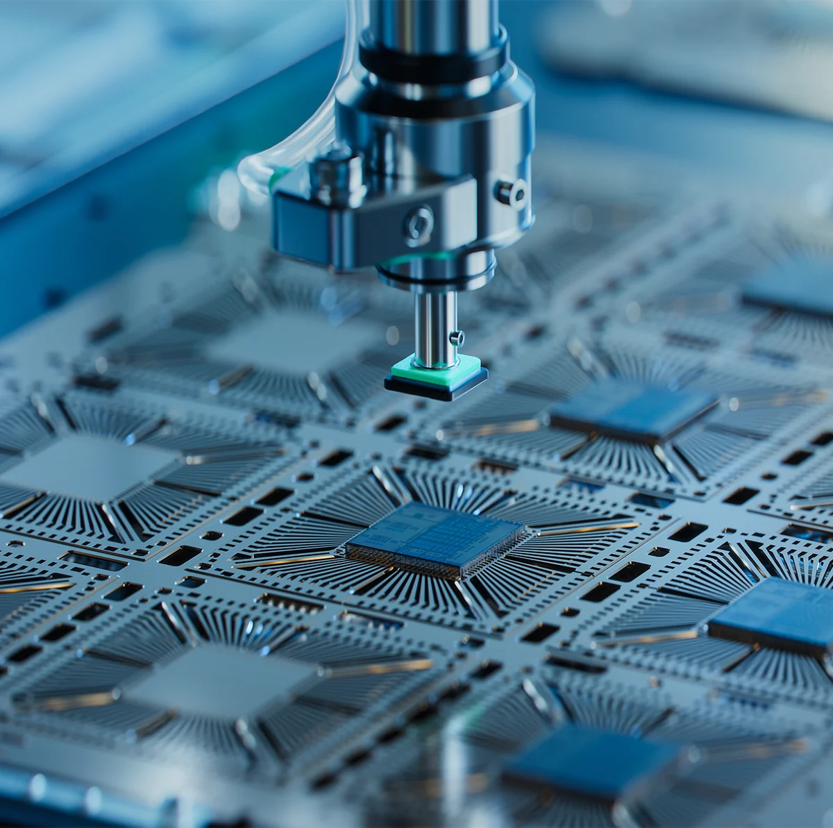
Package Assembly
Package assembly is a vital process in semiconductor manufacturing, where the semiconductor die is encapsulated in a protective package to ensure both durability and functionality.
During package assembly, electrical connections are established between the die and package leads, often using techniques such as wire bonding or flip-chip. In recent years, sintering solutions have gained prominence as an advanced bonding method within package assembly.
The integration of sintering solutions in package assembly offers several advantages, especially in high-performance applications where thermal management and electrical conductivity are critical. Sintering creates a robust, low-resistance joint between the die and the package, which enhances the overall performance and reliability of the semiconductor.
As part of package assembly, sintering solutions are used not only to attach the die to the package but also to form reliable interconnections between stacked die in advanced packaging technologies like 3D ICs or Package-on-Package (PoP) configurations.
Discover our sintering solutions
Read moreRelated products & services
ECOREL SINTEC AP90
ECOREL SINTEC AP90D
ECOREL SINTEC XP95
ECOREL SINTEC XP95D
Technical support
Inventec has a worldwide dedicated Technical Support team to help you along the different stages of our cooperation.
Depending on your request, we provide online or onsite support
- to select the right product based on your specific needs
- to assist you in your product qualification process
- to guide you with the initial set up of you process at all your worldwide manufacturing facilities
- to provide fast response on technical issues which could occur at any time during mass production.


Free-of-Charge cleaning & coating trials
Do you need cleaning or coating after soldering? We provides FREE-OF-CHARGE cleaning or coating trials in our Technical Centers. A comprehensive technical report detailing all test results and recommendations regarding process & process parameters will be provided. You want to attend the trials? We are happy to welcome you.